MicroSET: new machine for laser processing of materials applied in the electronic engineering industry
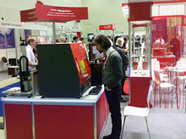
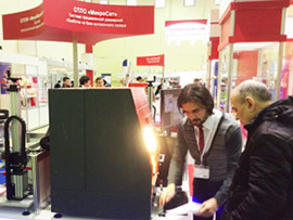
Laser Center enables specialists, engaged in production of electrical engineering, to see MicroSET machine in operation and get some expert advice at Stand 3D10 at the Photonics. World of Lasers and Optics 2015 trade show. The show was opened on March, 16 in Pavilion No.3 of Expocentre Fairgrounds.
The method of precision control of thermal field during laser materials processing was implemented in MicroSET machine made by Laser Center. This method allows solving various process tasks in the field of dimensional laser materials processing used in electrical engineering.
Modern lasers ensure high accuracy of spatiotemporal properties of single-mode laser beam at a wide range. These properties, along with an opportunity of high-precision (to the micron level) and fast (10-20 meters per second) control of the motion of the focused laser beam in space, create new opportunities to develop technologies based on control of thermal field in the material. Just recently using this method, we have developed technology and equipment for cutting sheet metals and alloys using low-power pulse lasers, technology and equipment for 3D metal engraving, technology and equipment for ultrafast laser hole drilling in metals and alloys.
The method of precision control of thermal field in the material reveals special advantages for technology and equipment for laser materials processing used in electronic engineering. Actually, to make electronic components one uses rather СexoticТ materials as regards laser processing techniques. Poly and mono crystals of semiconductors (silicon, gallium arsenide, etc.), ceramic materials based on aluminium oxide and silicon, various nitrides, carbides, precious metals, and alloys. Thermal gradients exert a detrimental effect on the materials, which is inevitable during production operation. Moreover, electrical engineering often requires processing of components made of biomaterials, e.g., when making elements for printed circuit boards based on alundum ceramics with copper coating. The tasks listed above cannot be solved using common methods of laser processing because thermal fields developed during processing cause distortions and failures. Processing of multicomponent materials is practically impossible, since processing of one coating causes damage to another one.
The method of precision control and development of thermal fields with desired properties provides nearly boundless opportunities to develop laser materials processing operations.
We have developed technology for flawless contour laser cutting of polycrystalline silicon and other semiconductors, technology for cutting ceramic materials, technology for ultrafast laser hole drilling in ceramic and other materials, technology for drilling shaped holes and mesostructures, laser technology for demetallization and manufacturing ceramic-based printed circuit boards, creation of high-resolution topology, making line targets, resistor trimming, and others.
We will be glad to see you on 16-19 March 2015 at Stand 3D10 in Pavilion No.3 of Expocentre Fairgrounds in Moscow.
For more information about our products go to Laser Center website www.newlaser.ru